Прецизионная инженерия у вас под рукой: полный анализ принципов конструкции мембранных переключателей
Аннотация:
В этой статье глубоко анализируются основные принципы конструкции мембранных переключателей, раскрывая их многослойную прецизионную конструкцию от красивых панелей до надежных схем. Анализируя панельный слой, слой заднего клея, слой схемы, слой поверхностного клея и общую интегрированную логику, он показывает материаловедение и инженерную мудрость, стоящую за его легкостью, тонкостью и надежностью, помогая вам полностью понять этот ключевой интерфейс взаимодействия человека и компьютера современных электронных устройств.
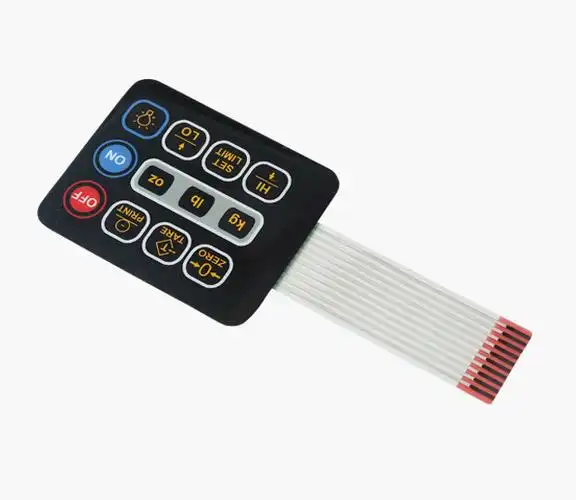
1. Панельный слой: первый интерфейс между функцией и эстетикой
Панельный слой - это "лицо", с которым пользователи непосредственно контактируют, обычно с использованием высокопрозрачных материалов, таких как ПЭТ или ПК, толщиной менее 0,25 мм. Его основная ценность заключается в:
- Высокая светопроницаемость: Обеспечьте равномерную передачу подсветки и улучшите визуальное восприятие (например, ночная работа медицинских устройств).
- Сильная адгезия: Точно напечатанный текст значков остается четким и не отпадает после миллионов нажатий.
- Гибкий и прочный: Ударопрочность материалов ПК может достигать 250 раз по сравнению с обычным стеклом, что обеспечивает надежность в экстремальных условиях.
Выбор материала напрямую определяет срок службы продукта и удобство использования, например, панели управления аэрокосмическим оборудованием должны выдерживать резкие перепады температуры от -70℃ до 150℃.
2. Клеевой слой: невидимый вклад в стабильное соединение
Клеевой слой - это "конструкционный клей" между мембранным переключателем и корпусом устройства, и выбор должен строго соответствовать характеристикам подложки:
- Общая среда: Общий двухсторонний клей обеспечивает экономичное решение для склеивания.
- Сценарий высокой надежности: Лента 3M VHB™ обладает сверхвысокой устойчивостью к атмосферным воздействиям и прочностью на отслаивание>40 Н/см (ссылка: Промышленное клеевое решение 3M).
- Особые потребности: Водонепроницаемый клей остается герметичным в среде с влажностью>90%, отвечая стандарту защиты IP67 для наружного оборудования.
3. Слой схемы (верхний/нижний слой): прецизионный носитель проводящей сети
Слой схемы - это "нервный центр" переключателя, с ПЭТ-пленкой 0,05-0,175 мм в качестве подложки:
- Проводящая серебряная паста: Квадратное сопротивление <0,1 Ом/□, используется для высокоточной передачи сигнала (ссылка: Технология проводящих чернил DuPont).
- Проводящая углеродная паста: Более низкая стоимость, отличная гибкость, подходит для изогнутых переключателей с радиусом кривизны >5 мм.
- Печать на микронном уровне: Точность ширины линии ±0,05 мм, обеспечивающая надежность проводимости контакта >1 миллиона раз.
4. Поверхностный клеевой слой: динамический барьер для герметизации и соединения
Поверхностный клеевой слой - это "адаптивное уплотнительное кольцо" между панелью и схемой, толщиной всего 0,05-0,15 мм:
- Высокая адгезия: Прочность на отслаивание >5 Н/см, исключающая расслоение между слоями.
- Защита окружающей среды: Химически стойкий клеевой слой может противостоять коррозии от спирта, разбавителей и т.д.
- Буфер напряжения: Модуль упругости 1–3 МПа, поглощает ключевые удары для защиты цепей, например, вибрационная среда центральной консоли автомобиля.
5. Интеграция ламинирования: совместное искусство прецизионной упаковки
Точное компаундирование многослойных структур определяет конечную производительность:
- Выравнивание на микронном уровне: Ошибка регистрации каждого слоя <0,1 мм, чтобы избежать смещения контакта.
- Устранение пузырьков: Технология вакуумного ламинирования обеспечивает отсутствие дефектов на поверхности склеивания.
- Горячее прессование: Давление равномерно прикладывается при температуре 130℃±5℃ для обеспечения постоянной прочности склеивания по всей площади.
6. Конструкция контакта: интеллектуальная эволюция механизма проводимости
От физического контакта к инновациям в технологии индукции:
- Арочная пружина: Ход 0,2–0,5 мм, обеспечивает четкую тактильную обратную связь (срок службы клавиш > 5 миллионов раз).
- Емкостное зондирование: ITO-покрытие обеспечивает бесконтактное срабатывание, подходит для сценариев асептической работы.
- Резистивная матрица: Точное расположение осей X/Y, поддерживающее сложный многоточечный интерфейс управления.
Заключение: Грандиозная инновация в микро-слоях
При общей толщине менее 1 мм, мембранные переключатели объедините междисциплинарную мудрость полимерных материалов, прецизионной печати и электронной инженерии. От панелей со светопропусканием >90% до схем, выдерживающих 100 000 изгибов, от проводящих путей из нано-серебряной пасты до склеивания и герметизации на микронном уровне – инновации на каждом слое переопределяют границы взаимодействия человека и компьютера. Когда кончики пальцев касаются переключателя, за этим, казалось бы, простым действием стоит точный танец материаловедения, структурной механики и электронной техники. С ростом гибкой электроники и носимых устройств легкие, тонкие и прочные характеристики мембранных переключателей будут продолжать лидировать в интерактивной революции, позволяя технологиям более органично интегрироваться в жизнь человека.
Его ценность заключается не только в проведении цепей, но и в использовании миллиметровой точности укладки для построения невидимого моста между человеческими намерениями и цифровым миром в небольшом пространстве.